| Place of Origin: | China |
|---|---|
| Brand Name: | Kingsum Electronic |
| Certification: | UL&ROHS |
| Model Number: | Kingsum ElectronicA-007 |
| Minimum Order Quantity: | 1 Unit |
|---|---|
| Packaging Details: | P/P |
| Delivery Time: | 10 ~ 20 wprking days |
| Payment Terms: | T/T, Western Union, MoneyGram, L/C, D/A |
| Supply Ability: | 2000 m2 / Month |
| Layer Count: | 2 ` 30 Layers | Max Board Size: | 600 Mm X 1200 Mm |
|---|---|---|---|
| Base Material For PCB: | FR4, CEM-1, TACONIC, Aluminium, High Tg Material, High Frequence ROGERS ,TEFLON, ARLON, Halogen-free Material | Rang Of Finish Baords Thickness: | 0.21-7.0mm |
| Minimum Line Width: | 3mil (0.075mm) | Minimum Line Space: | 3mil (0.075mm) |
| Minimum Hole Diameter: | 0.10 Mm | Finishing Treatment: | HASL (Tin-Lead Free), ENIG(Immersion Gold), Immersion Silver , Gold Plating (Flash Gold), OSP, Etc. |
| Thickness Of Copper: | 0.5-14oz (18-490um) | E-Testing: | 100% E-Testing (High Voltage Testing); Flying Probe Testing |
| High Light: | fr4 printed circuit board,multilayer circuit board | ||
1. Features of Bluetooth PCBA
• Material: FR4 Tg180, 6-layer
• Minimum trace/space: 0.1mm
• Blind and buries via and via in pad
Material: FR4, high Tg
RoHS Directive-compliant
Board thickness: 0.4-5.0 mm +/-10%
Layer count: 1-22 layers
Copper weight: 0.5-5oz
Min finish hole side: 8 mils
Laser drill: 4 mils
Min trace width/space: 4/4 mils (production), 3/3 mils (sample run)
Solder mask: green, blue, white, black, blue and yellow
Legend: white, black and yellow
Max board dimensions: 18*2 inches
Finish type options: gold, silver, tin, hard gold, HASL, LF HASL
Inspection standard: ipc-A-600H/IPC-6012B, class 2/3
Electronic test: 100%
Report: final inspection, E-test, solder ability test, micro section
Certifications: UL, SGS, RoHS Directive-compliant , ISO 9001:2008, ISO/TS16949:2009
2. Bluetooth PCBA capability
| SMT | Position accuracy:20 um |
| Components size:0.4×0.2mm(01005) —130×79mm,Flip-CHIP,QFP,BGA,POP | |
| Max. component height::25mm | |
| Max. PCB size:680×500mm | |
| Min. PCB size:no limited | |
| PCB thickness:0.3 to 6mm | |
| PCB weight:3KG | |
| Wave-Solder | Max. PCB width:450mm |
| Min. PCB width: no limited | |
| Component height:Top 120mm/Bot 15mm | |
| Sweat-Solder | Metal type :part, whole, inlay, sidestep |
| Metal material:Copper , Aluminum | |
| Surface Finish:plating Au, plating sliver , plating Sn | |
| Air bladder rate:less than20% | |
| Press-fit | Press range:0-50KN |
| Max. PCB size:800X600mm | |
| Testing | ICT,Probe flying,burn-in,function test,temperature cycling |
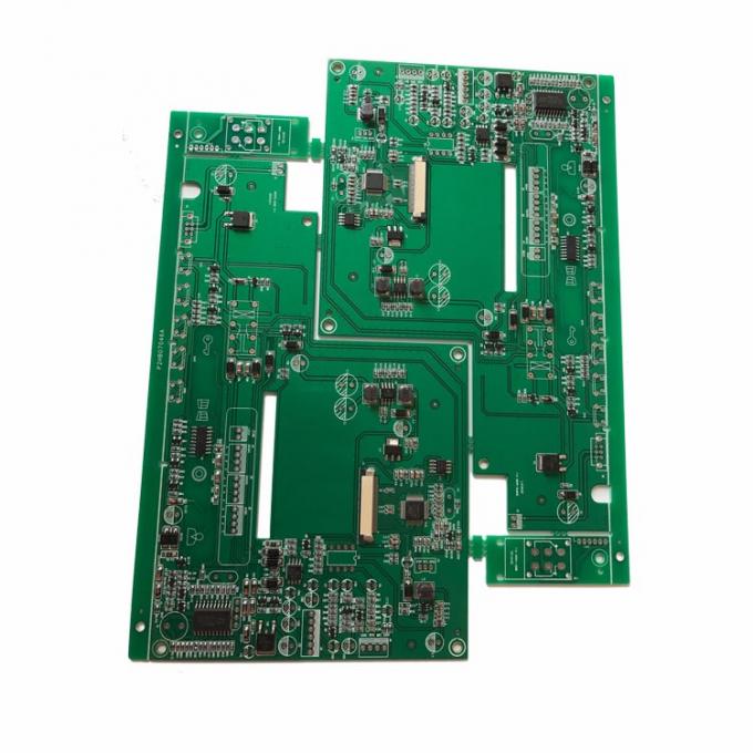
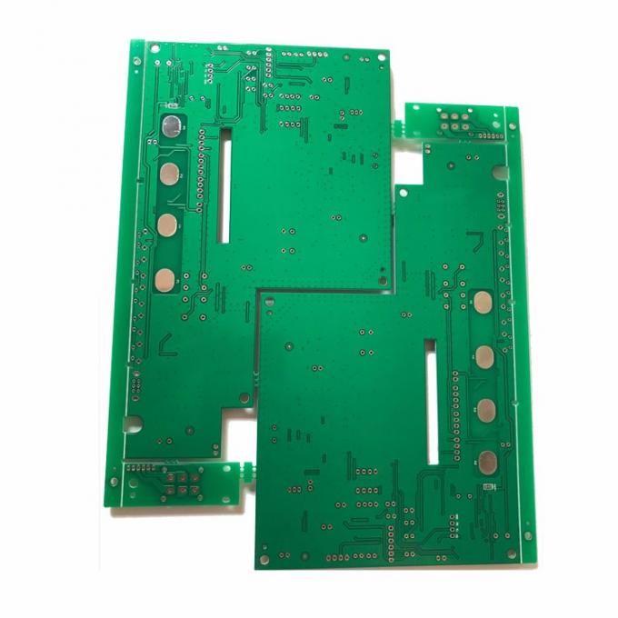
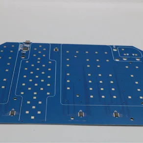
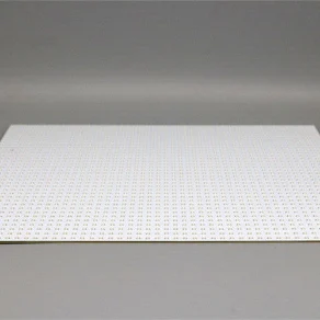
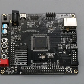
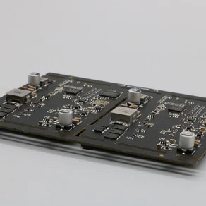
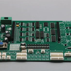
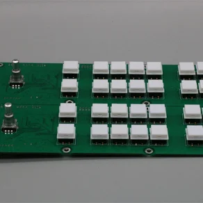
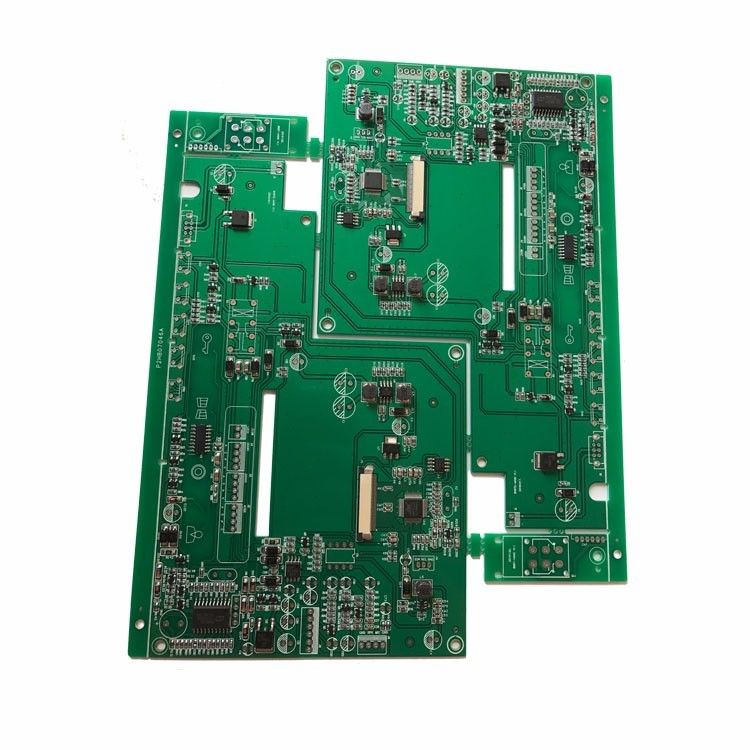
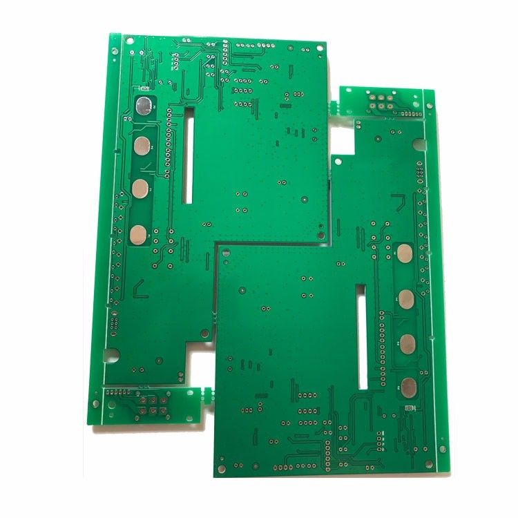
3. Bluetooth PCBA Pictures